filmov
tv
Advanced Process Nodes
0:03:49
Enabling USB 2.0 in Advanced Process Nodes Using DesignWare eUSB2 IP | Synopsys
0:15:00
DAC Innovation Theater - Design for Advanced Process Nodes
0:32:25
SoC Design Methodology Challenges for Advanced Process Nodes
0:13:57
What is wrong with 5nm, 3nm, 1nm.. CPU Technology Nodes explained
0:59:06
On Chip AI, Hardware Security, and Trust Using Advanced Process Nodes Dr Rashmi Jha, July 23, 20
0:05:11
EDA Enables Advanced Designs at All Process Nodes | Synopsys
0:02:05
Semiconductor production process explained
0:05:35
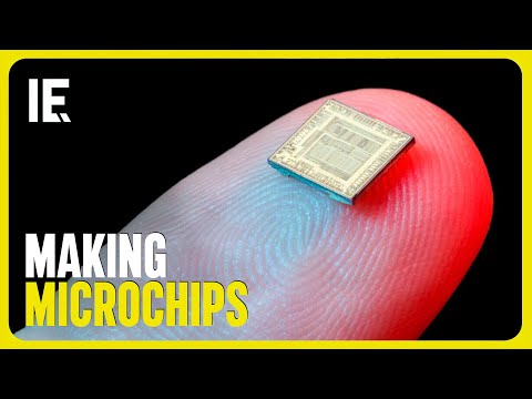
💻 How Are Microchips Made?
0:16:02
How to setup XProtocol Xardian Node on a VPS (Linux OS)
0:02:10
In-design Electrical Reporting Process for Samsung Foundry Advanced Nodes | Synopsys
0:12:46
Electromigration And IR Drop At Advanced Nodes
0:04:25
What are Geometry Nodes?
0:48:11
Geometry Nodes development process
0:06:21
Hadoop In 5 Minutes | What Is Hadoop? | Introduction To Hadoop | Hadoop Explained |Simplilearn
0:16:59
How AMD Left GlobalFoundries for TSMC
0:13:39
China's 7nm Chips: SMIC N+2
0:03:25
Applications Designed for Established and Emerging Nodes | Synopsys
0:05:45
Neural Network In 5 Minutes | What Is A Neural Network? | How Neural Networks Work | Simplilearn
0:24:09
Blender for Scientists - Advanced Geometry Nodes Part 1 - Variables
0:06:00
How Do CPUs Use Multiple Cores?
0:17:47
Even and Odd and Advanced Selections with MODULO in Blender - Geometry Nodes
0:29:21
Understanding Nodes in Color Grading // Davinci Resolve 18
0:18:36
Understanding the Finite Element Method
0:14:23
Debug Changes At Advanced Nodes
Вперёд
 0:03:49
 0:15:00
 0:32:25
 0:13:57
 0:59:06
 0:05:11
 0:02:05
 0:05:35
 0:16:02
 0:02:10
 0:12:46
 0:04:25
 0:48:11
 0:06:21
 0:16:59
 0:13:39
 0:03:25
 0:05:45
 0:24:09
 0:06:00
 0:17:47
 0:29:21
 0:18:36
 0:14:23